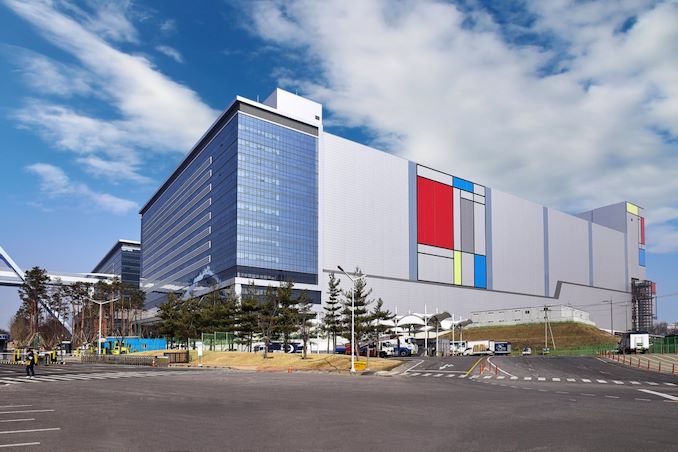
Samsung Foundry has started mass production of chips using its 6LPP and 7LPP manufacturing processes at its new V1 fab. The new facility employs one of the industry’s first production lines built from the ground up for technologies that heavily use EUV tools.
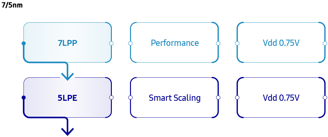
EUVL is a key enabler for Samsung’s next-generation leading-edge fabrication processes as it allows to reduce usage of multipatterning, and increases yields of chips architected for smaller technologies. Samsung currently uses EUVL equipment for its 6LPP and 7LPP nodes, and will expand its usage in future nodes such as 5LPE, 4LPE, 3GAE, and 3GAP processes.
Samsung Foundry’s 7LPP and 6LPP process technologies are used to make advanced mobile SoCs that will be shipped in Q1. The contract manufacturer of semiconductors does not disclose names of its client(s), but it is noteworthy that its 6LPP technology is not a part of its MPW (multi project wafer) shuttle program, which may indicate that the process is only available for Samsung itself and/or select customers who do not use MPWs.
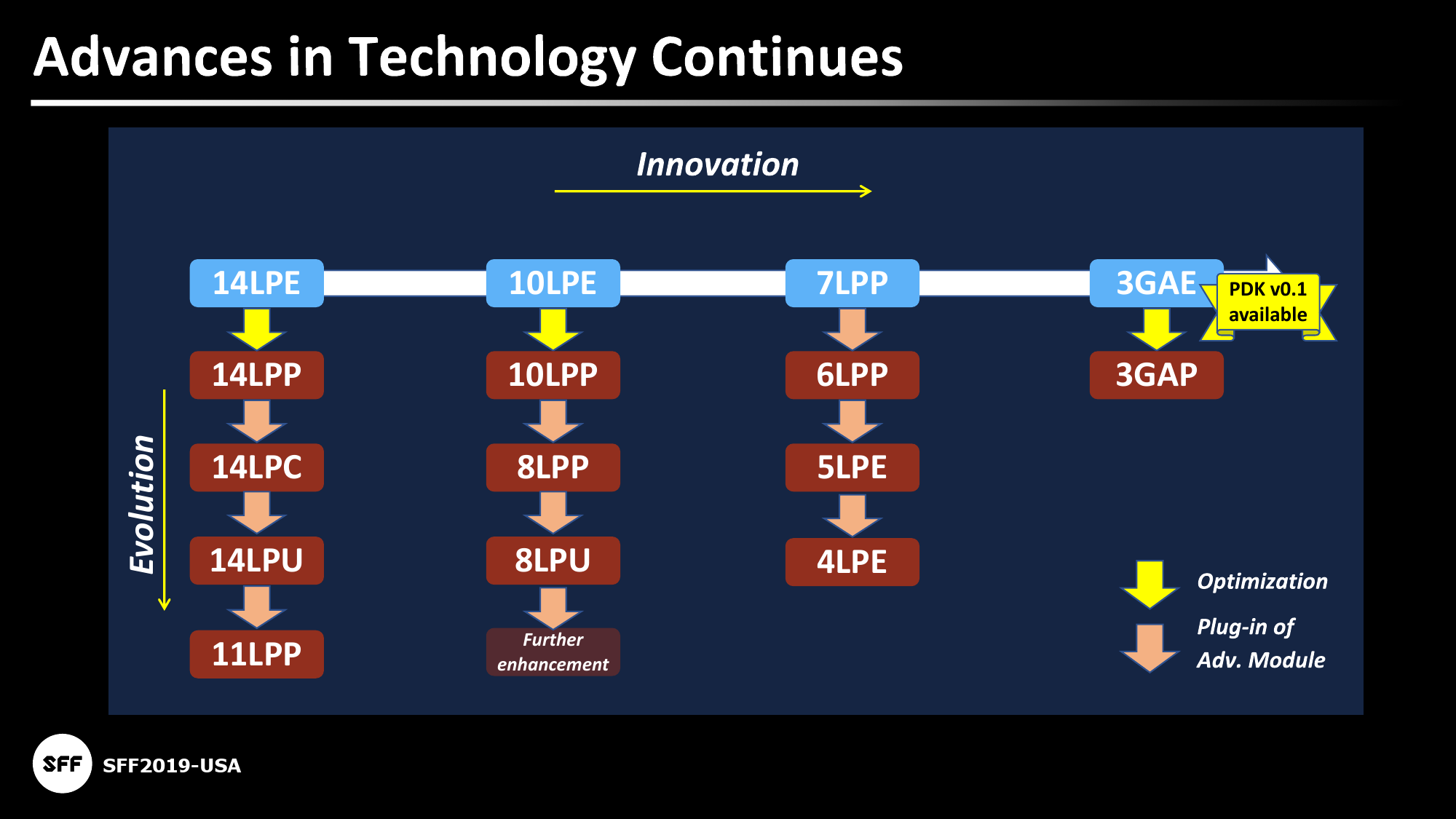
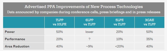
Samsung’s 6LPP is a evolution of its 7LPP node that offers slightly higher (~10%) transistor density and lower power, but is compatible with, and can reuse IP initially developed for 7LPP. Furthermore, 6LPP supports smart structures for designers eager to invest in all-new IP, as well as multi diffusion break feature. Meanwhile, 5LPE promises to bring further advantages when it comes to power, performance, when compared to 6LPP.
6LPP looks to be a limited offer node for select customers, whilst Samsung's focus in the future looks to be on its new 5LPE node.
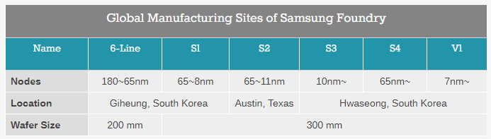
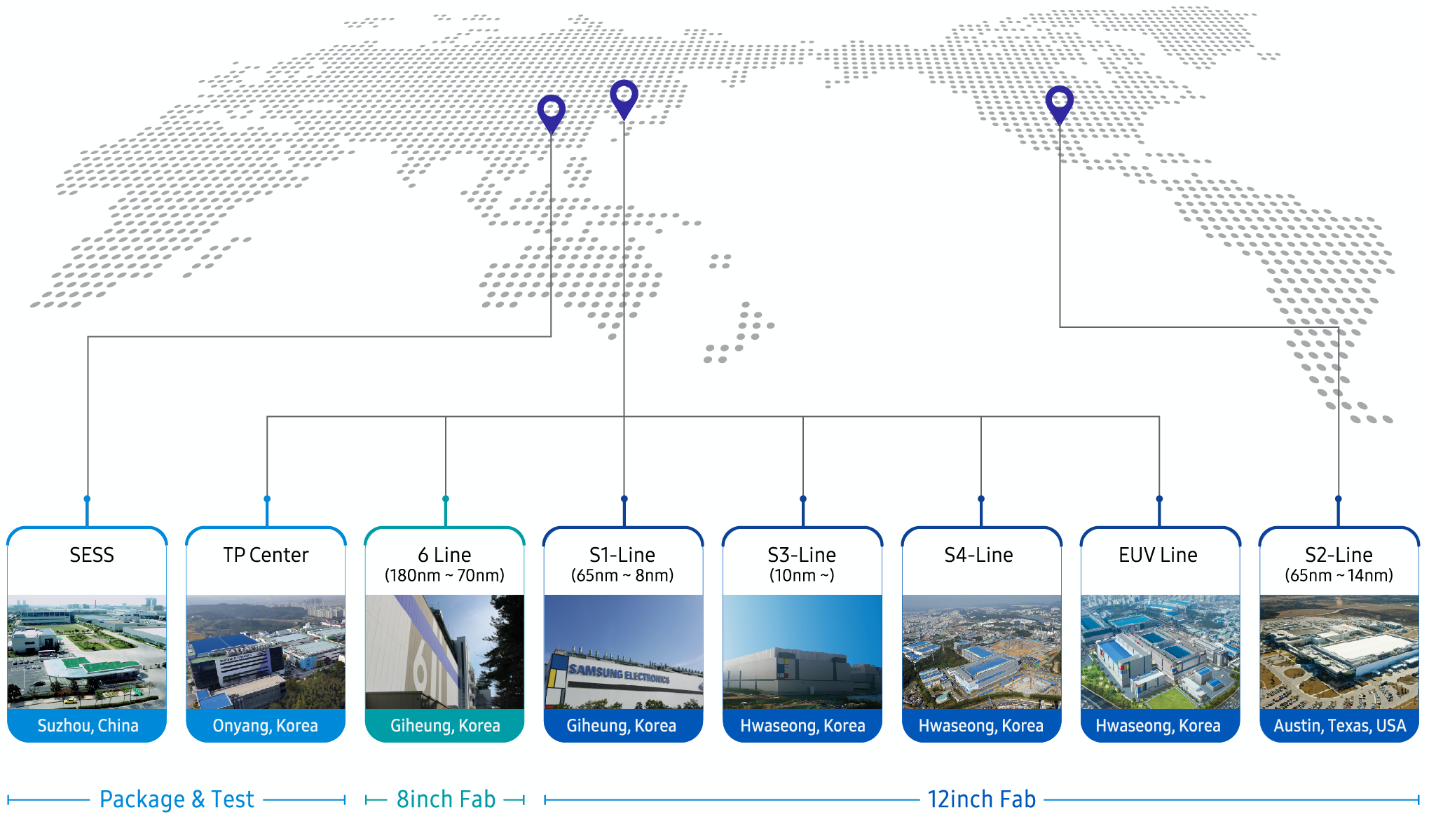
Samsung’s V1 fab is located in Hwaseong, Korea, adjacent to its S3 line, where Samsung started initial ramp of chips made using its 7LPP technology. The company began construction of V1 in February 2018, and initiated test wafer production in the second half of 2019. Samsung continues to ramp up its V1 fab now and says that by the end of the year its total capacity for EUV-enabled 7LPP and below nodes will be three times higher than it was in 2019. Meanwhile, cumulative investments in the V1 line will hit $6 billion by the end of 2020.